- Nederlands, Belgique / België
- Česky, Česká republika
- Deutsch, Deutschland
- Español, España
- English, Europe
- Français, France
- Italiano, Italia
- Magyar, Magyarország
- Nederlands, Nederland
- Deutsch, Österreich
- Polski, Polska
- Română, România
- Français / Deutsch, Suisse / Schweiz
- Svenska, Sverige
- Suomeksi, Suomi
- Türkçe, Türkiye
- English, United Kingdom
- Slovenská, Slovak
- Español, Mexico


 Welkom bij Mitutoyo Nederland, België en Danmark

- Alle Product Highlights
- Measurlink 10
- HR-600 Series
- TAGLENS
- MCOSMOS 5
- Crysta Apex V
- Formtracer Avant
- MiSTAR 555
- Calipers
- Bluetooth Data Transmission
- PJ Plus
- QuickVision Pro
- Alle Producten per Industrie
- MeasurLink 10
- MeasurLink 10
- Medical
- Automotive
- Aerospace
- Energy
- Gen. Manufacturing
- Electronics
- Case Studies
- Alle Handmeetgereedschappen
- Schuifmaten
- Schroefmaten
- Binnenmeetinstrumenten
- Diepte meetinstrumenten
- Hoogtemeters
- Meetklokken en Snelopnemers
- Hulpstukken en diverse
- Kalibratie instrumenten
- Eindmaten
- Alle CMM
- Kleine en middelgrote CMM's
- CMMs met grote afmetingen
- In-Line en werkvloer CMMs
- CMM Tastsystemen
- Styli en accessoires
- Opspansystemen
- KMG behuizing
- CMM Software
- Alle Vision
- 2D Vision Meetsystemen Quick Image
- Manueel 3D Vision Meetsystemen Quick Scope
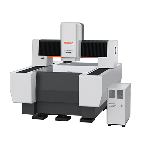
- 3D CNC Vision Meetsystemen Quick Vision
- 3D CNC Multisensor Meetsystemen Quick Vision
- Serie 365 - CNC Visionmeetsysteem
- 3D CNC Meetsystemen voor Micro Geometrieën
- Vision System Software
- Objectieven en kalibratiekaarten
- Alle Optisch
- Magnifiers
- Measuring Projectors
- Measuring Microscopes
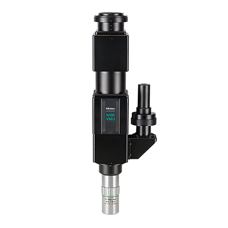
- Microscope Units
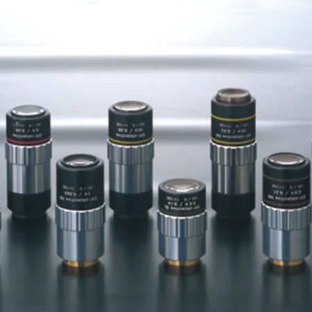
- Objective Lenses
- TAGLENS
- Illumination Units
- Alle Hardheid
- Portable Hardness Testers
- Combination Testers
- Vickers Testers
- Automatic Vickers Testers
- Micro-Vickers Testers
- Hardness Testing Software
- Reference materials and indenters
- Alle Sensoren
- Linear Gauges
- Low Force Gauges
- Counters and Display Units
- Laser Scan Micrometers
- Surface Measure
- Sensor Management Software
- Schuifmaten
- Digitale schuifmaten
- Schuifmaten voor speciale doeleinden
- Analoge schuifmaten
- Schuifmaat accessoires
- Schroefmaten
- Digimatic schroefmaten & Analoge schroefmaten
- Accessoires voor schroefmaten
- Inbouwschroefmaten
- Accessoires voor inbouwschroefmaten
- Binnenmeetinstrumenten
- Binnenmeetinstrumenten
- Binnenmeettasters
- Accessoires voor binnenmeetinstrumenten
- Meetklokken en Snelopnemers
- Digital Indicators
- Accessoires voor meetklokken
- Zwenktaster
- Meetklok
- Accessoires voor meetklokken
- Diktemeter, dieptemeter
- Eindmaten
- Stalen eindmatensets
- Stalen losse eindmaten
- CERA eindmatensets
- CERA keramische losse eindmaten
- Speciale eindmaten
- Accessoires voor eindmaten
- Kleine en middelgrote CMM's
- CRYSTA-Apex V - 500, 700, & 900 Series
- CRYSTA-Apex V - 1200 Series
- CRYSTA-Apex V - 1600 & 2000 Series
- CRYSTA-Apex EX Series for REVO
- STRATO-Apex - 500, 700, & 900 Series
- STRATO-Apex - 1600 Series
- LEGEX Series
- Styli en accessoires
- Styli Kits
- Straight Styli
- Diamond Coated Styli
- Master Ball
- Machine Tool Styli
- Star Styli
- Styli for Star Styli
- Cylinder Styli
- Disk Styli
- Tip Styli
- Extensions
- Holders
- Adapters
- Joints
- Screws for Cubes
- Tools
- StyliCleaner
- Opspansystemen
- Fixturing Kits
- Base Plates
- Build-up Components
- Positioning & Stopper Components
- Profile Components
- Base Components
- Clamping Components
- Adapters
- Slider Components
- Racks
- 3D CNC Vision Meetsystemen Quick Vision
- Quick Vision ACTIVE
- Quick Vision APEX / HYPER
- Quick Vision ACCEL
- Quick Vision ULTRA
- Measuring Projectors
- PJ Series
- PV Series
- PH Series
- M2 Software
- Data Processing Unit
- Edge Detection Sensor
- Accessories
- Measuring Microscopes
- TM Series Gen. B
- MF Series Gen. D
- MF-U Series Gen. D
- Illumination Sources
- Hyper MF Series
- Vision Unit
- M2 Software
- QSPAK-VUE Software
- Objective Lenses
- ML-Series Objectives
- Brightfield Observation Objectives
- Brightfield/Darkfield Observation Objectives
- NIR Objectives
- NIR LCD Objectives
- NUV Objectives
- NUV LCD Objectives
- UV Objectives
- UV LCD Objectives
- Oppervlakte ruwheid
- Surftest SJ-210
- Surftest SJ-310
- Surftest SJ-410
- Surftest SJ-500
- Surftest SV-2100
- Surftest SJ-500P
- Surftest SV-2100P
- Formtracer Avant FTA-S3000
- Surftest Extreme SV-3000CNC
- Surftest Extreme SV-M3000CNC
- Oppervlakte ruwheid & Contour
- Formtracer Avant FTA-D3000 / FTA-D4000 Series
- Formtracer CS-3300
- Formtracer Extreme SV-C4500CNC
- Formtracer Extreme SV-C4500CNC HYBRID Type 1
- Formtracer Extreme CS-5000CNC and CS-H5000CNC
- Portable Hardness Testers
- Impact Type Hardness Testing Unit HARDMATIC HH-411
- Digital and Analogue Durometers HARDMATIC HH-300
- Combination Testers
- Rockwell HR-200/300/400
- Rockwell, Rockwell Superficial, Brinell Hardness Tester HR-530 and HR-600
- Rockwell Automatic Hardness Testing HR-600
- Automatic Vickers Testers
- Automatic Micro-Vickers hardness testing systems
- Automatic Vickers hardness testing systems
- Reference materials and indenters
- Hardness reference materials
- Hardness indenters and replacement balls
- Linear Gauges
- ABSOLUTE Digimatic Linear Gauge LGS Series
- Air Drive Unit
- ABSOLUTE Digimatic Linear Gauge LGD Series
- Standard Linear Gauge LGF Series
- Linear Gauge LG100 Series
- Linear Gauge LG200 Series
- Slim Head Linear Gauge LGK Series
- Slim Head Linear Gauge LGB Series
- Large Measuring Range Linear Gauge LG
- Laser Hologauge
- Counters and Display Units
- EJ Counter and Interfaces for Linear Gauges
- EC Counter for Linear Gauges
- EG Counter for Linear Gauges
- EB Counter for Linear Gauges
- EH Counter for Linear Gauges
- EV Counter for Linear Gauges
- Display Unit for EV Counter
- Laser Scan Micrometers
- Laser Scan Micrometer Measuring Unit and Display Unit Package
- Laser Scan Micrometer Measuring Unit
- Laser Scan Micrometer
- Laser Scan Micrometer Display Unit
- Laser Scan Micrometer Optional Accessories
- DRO Linear Scales and Counters
- DRO Linear Scales AT103
- DRO Linear Scales AT103 - High Accuracy
- DRO Linear Scales AT113
- DRO Linear Scales AT113 - High Accuracy
- DRO Linear Scales AT116
- DRO ABS Linear Scales AT715
- Universal DRO KA-200 Counter
- NC Linear Scales
- NC Linear Scales ST36
- NC Linear Scales ST46-EZA
- NC Linear Scales ABS ST700
- NC Linear Scales ABS ST1300
- NC Linear Scales AT211
- NC Linear Scales ABS AT1100
- NC Linear Scales ABS AT1300
- NC Linear Scales AT402E
- NC Linear Scales AT203
- NC Linear Scales AT402E with cable A/B
- NC Linear Scales AT402E with cable C
- Scale Units
- Horizontal ABSOLUTE Scale Coolant Proof IP66
- Horizontal ABSOLUTE Scale Standard
- Horizontal ABSOLUTE Scale Measurement Direction Switching
- Horizontal ABSOLUTE Scale Diameter Function
- Vertical ABSOLUTE Scale Standard
- Vertical ABSOLUTE Scale Measurement Direction Switching
- Vertical ABSOLUTE Scale Diameter Function
- Signal Cables
- USB Input Tool Direct (Digimatic-USB Cable)
- Digimatic Data Cables
- Digimatic Extension Cables
- Wireless Communication
- Wireless Communication System U-WAVE
- U-WAVE Bluetooth
- U-WAVE-T Connection Cables and Connection Units
- Interfaces
- USB Input Tool
- DMT-3T / FS2 USB
- DMX-1 USB
- DMX-2 S
- DMX-2 USB
- DMX-3 USB
- MUX-10F
- DMX-8/2
- DMX-16 / DMX-16C
- DMX-0-1 USB / DMX-3-2 USB
- Digimatic Interface MIG
 Original Equipment Manufacturers (OEM)
Mitutoyo OEM kan ontbrekende expertise of middelen aanpakken door u onze befaamde meetapparatuur te leveren die naadloos integreert in uw producten.
 Luchtvaart
Complexe lucht- en ruimtevaarttoepassingen hebben snelle, uiterst nauwkeurige kwaliteitscontrole nodig om nauwkeurige assemblages te garanderen. Zie hoe Mitutoyo dit mogelijk maakt
 Auto industrie
De auto-industrie blijft innoveren en Mitutoyo levert de geavanceerde inspectie- en scanmogelijkheden om fabrikanten te helpen bij het realiseren van een continue productie.
 Energie
De meet- en analyseoplossingen van Mitutoyo zijn ontworpen om energieleveranciers te helpen hun betrouwbaarheid te verbeteren en de uptime van hun apparatuur te verhogen.
 Medisch
Om het welzijn van patiënten te beschermen, vereisen medische toepassingen uitzonderlijke nauwkeurigheid. Bekijk hoe uitgebreid geteste oplossingen van Mitutoyo u kunnen helpen dit te bereiken.
 Maak industrie
Zorg voor een hoge herhaalbaarheid en strenge kwaliteitscontrole met oplossingen voor vormmetingen, coördinatenmeetmachines en precisiemeetgereedschap van Mitutoyo.
 Semiconductor
De contactloze en vision meetoplossingen van Mitutoyo brengen microscopische nauwkeurigheid naar kleinere en dichtere elektronische componenten.
 Case Studies
Voor een overzicht van de mogelijkheden van Mitutoyo is er geen betere plek dan onze prachtige verzameling casestudy's.
 Helpdesk Support
Perfecte en probleemloze installatie en integratie in uw IT-infrastructuur.
 Field Services
On-site service van uw favoriete meet- en testmachines
 Kalibratie Services
Laat je meetapparatuur kalibreren door een laboratorium dat je vertrouwt
 Meetservices
Get your workpieces and parts measured from anywhere in Europe
 Reparaties & Reserve onderdelen
Reserveonderdelen en reparaties voor Mitutoyo-apparaten
 Smart Factory Oplossingen
Maak van uw fabriek een slimme fabriek met de hulp van Mitutoyo
 Education Pack
Er is geen betere hulp dan posters of lesmateriaal van Mitutoyo, perfect voor de werkplaats of het klaslokaal.
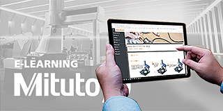 E-Learning
Voor degenen die geïnteresseerd zijn in metrologie biedt Mitutoyo E-Learning-cursussen om studenten, personeel of zelfs hobbyisten op te leiden.
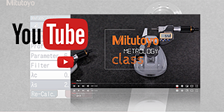 Online Material
Als je op zoek bent naar een snelle manier om meer te leren over meten, bekijk dan onze vele instructievideo's

 Ontdek Mitutoyo
Het grootste metrologiebedrijf ter wereld
 Merchandise
Voor degenen die in stijl over de winkelvloer willen lopen, ga naar de shop en steun je favoriete merk.
 Mitutoyo Danmark
Læs alt om Mitutoyo Danmark her


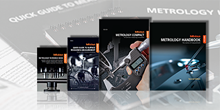
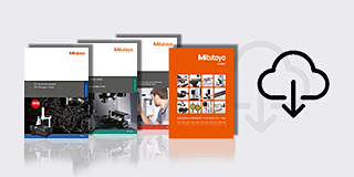 Product informatie
Bekijk en download onze catalogus, productbrochures en meer
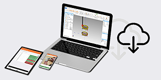 Software
Download onze software en updates eenvoudig en gemakkelijk
 Verklaringen van conformiteit
Hier kun je de volledige versies voor de EU en het VK downloaden
 Gratis wallpapers
Download hier gratis de officiële wallpapers van Mitutoyo
 Mitutoyo Merk Communicatie Materialen
Hulpmiddelen voor Mitutoyo-medewerkers en externe leveranciers
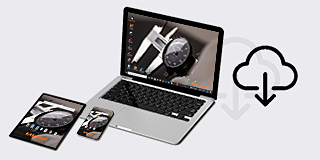
 Online Catalogus
Bekijk ons uitgebreide assortiment in onze online catalogus!
-
Producten
- Terug Producten
- Producten
- Product Highlights
-
Producten per Industrie
- Terug Producten per Industrie Alle Producten per Industrie
- MeasurLink 10
- MeasurLink 10
- Medical
- Automotive
- Aerospace
- Energy
- Gen. Manufacturing
- Electronics
- Case Studies
-
Handmeetgereedschappen
- Terug Handmeetgereedschappen Alle Handmeetgereedschappen
- Schuifmaten
- Schroefmaten
-
Binnenmeetinstrumenten
- Terug Binnenmeetinstrumenten Binnenmeetinstrumenten
- Binnenmeetinstrumenten
- Binnenmeettasters
- Accessoires voor binnenmeetinstrumenten
-
Diepte meetinstrumenten
- Terug Diepte meetinstrumenten Diepte meetinstrumenten
- Diepte schroefmaat
- Diepteschuitmaat
- Diepteschuifmaat accessoires
- Hoogtemeters
- Meetklokken en Snelopnemers
- Hulpstukken en diverse
-
Kalibratie instrumenten
- Terug Kalibratie instrumenten Kalibratie instrumenten
- Hoogteschroefmaat Height Master
- Stappeneindmaat
- Kalibratie apparatuur
- Eindmaten
-
CMM
- Terug CMM Alle CMM
- Kleine en middelgrote CMM's
-
CMMs met grote afmetingen
- Terug CMMs met grote afmetingen CMMs met grote afmetingen
- CARB-Series
-
In-Line en werkvloer CMMs
- Terug In-Line en werkvloer CMMs In-Line en werkvloer CMMs
- MACH Ko-ga-me
- MACH 3A 653
- MACH V 9106
- MiSTAR 555
-
CMM Tastsystemen
- Terug CMM Tastsystemen CMM Tastsystemen
- SurfaceMeasure
- REVO
- SP80
- TP7M
- PH20
- Styli en accessoires
- Opspansystemen
-
KMG behuizing
- Terug KMG behuizing KMG behuizing
- CMM Enclosures
-
CMM Software
- Terug CMM Software CMM Software
- MiCAT Planner
- MCOSMOS
- MAFIS Express
- MSURF
-
Vision
- Terug Vision Alle Vision
-
2D Vision Meetsystemen Quick Image
- Terug 2D Vision Meetsystemen Quick Image 2D Vision Meetsystemen Quick Image
- Quick Image
- Quick Image Software
-
Manueel 3D Vision Meetsystemen Quick Scope
- Terug Manueel 3D Vision Meetsystemen Quick Scope Manueel 3D Vision Meetsystemen Quick Scope
- Manual Quick Scope
- Quick Scope Software
-
3D CNC Vision Meetsystemen Quick Vision
- Terug 3D CNC Vision Meetsystemen Quick Vision 3D CNC Vision Meetsystemen Quick Vision
- Quick Vision ACTIVE
- Quick Vision APEX / HYPER
- Quick Vision ACCEL
- Quick Vision ULTRA
-
3D CNC Multisensor Meetsystemen Quick Vision
- Terug 3D CNC Multisensor Meetsystemen Quick Vision 3D CNC Multisensor Meetsystemen Quick Vision
- Quick Vision Hybrid
- Quick Vision WLI
-
Serie 365 - CNC Visionmeetsysteem
- Terug Serie 365 - CNC Visionmeetsysteem Serie 365 - CNC Visionmeetsysteem
- MiSCAN APEX 404
- MiSCAN HYPER 302
- MiSCAN HYPER 404
-
3D CNC Meetsystemen voor Micro Geometrieën
- Terug 3D CNC Meetsystemen voor Micro Geometrieën 3D CNC Meetsystemen voor Micro Geometrieën
- UMAP Vision Systems
- UMAP Software
- Vision System Software
- Objectieven en kalibratiekaarten
-
Optisch
- Terug Optisch Alle Optisch
- Magnifiers
-
Measuring Projectors
- Terug Measuring Projectors Measuring Projectors
- PJ Series
- PV Series
- PH Series
- M2 Software
- Data Processing Unit
- Edge Detection Sensor
- Accessories
- Measuring Microscopes
-
Microscope Units
- Terug Microscope Units Microscope Units
- Microscope Unit FS70 Series
- Video Microscope Unit VMU Series
- Objective Lenses
- TAGLENS
- Illumination Units
- Vorm
-
Hardheid
- Terug Hardheid Alle Hardheid
- Portable Hardness Testers
- Combination Testers
-
Vickers Testers
- Terug Vickers Testers Vickers Testers
- Vickers Hardness Testing Machine HV-110/120
- Automatic Vickers Testers
-
Micro-Vickers Testers
- Terug Micro-Vickers Testers Micro-Vickers Testers
- Micro-Vickers Hardness Testing Machines HM-210/220
-
Hardness Testing Software
- Terug Hardness Testing Software Hardness Testing Software
- AVPAK
-
Reference materials and indenters
- Terug Reference materials and indenters Reference materials and indenters
- Hardness reference materials
- Hardness indenters and replacement balls
-
Sensoren
- Terug Sensoren Alle Sensoren
-
Linear Gauges
- Terug Linear Gauges Linear Gauges
- ABSOLUTE Digimatic Linear Gauge LGS Series
- Air Drive Unit
- ABSOLUTE Digimatic Linear Gauge LGD Series
- Standard Linear Gauge LGF Series
- Linear Gauge LG100 Series
- Linear Gauge LG200 Series
- Slim Head Linear Gauge LGK Series
- Slim Head Linear Gauge LGB Series
- Large Measuring Range Linear Gauge LG
- Laser Hologauge
- Low Force Gauges
- Counters and Display Units
- Laser Scan Micrometers
-
Surface Measure
- Terug Surface Measure Surface Measure
- Surface Measure 1008S
- Accessories
- Sensor Management Software
-
Digital Scales
- Terug Digital Scales Alle Digital Scales
- DRO Linear Scales and Counters
-
NC Linear Scales
- Terug NC Linear Scales NC Linear Scales
- NC Linear Scales ST36
- NC Linear Scales ST46-EZA
- NC Linear Scales ABS ST700
- NC Linear Scales ABS ST1300
- NC Linear Scales AT211
- NC Linear Scales ABS AT1100
- NC Linear Scales ABS AT1300
- NC Linear Scales AT402E
- NC Linear Scales AT203
- NC Linear Scales AT402E with cable A/B
- NC Linear Scales AT402E with cable C
-
Scale Units
- Terug Scale Units Scale Units
- Horizontal ABSOLUTE Scale Coolant Proof IP66
- Horizontal ABSOLUTE Scale Standard
- Horizontal ABSOLUTE Scale Measurement Direction Switching
- Horizontal ABSOLUTE Scale Diameter Function
- Vertical ABSOLUTE Scale Standard
- Vertical ABSOLUTE Scale Measurement Direction Switching
- Vertical ABSOLUTE Scale Diameter Function
-
Data Management
- Terug Data Management Alle Data Management
-
Data Management Software
- Terug Data Management Software Data Management Software
- MeasurLink 10
- USB-ITPAK
-
Mini Processors
- Terug Mini Processors Mini Processors
- Digimatic Mini Processor DP-1VA LOGGER
- Signal Cables
- Wireless Communication
- Interfaces
-
Timerbox, Digimatic Switch Box, Tolerance Box
- Terug Timerbox, Digimatic Switch Box, Tolerance Box Timerbox, Digimatic Switch Box, Tolerance Box
- Digimatic Timerbox
- Digimatic Data Logger
- Digimatic Switch Box
- Digimatic Tolerance Box
-
Software
- Terug Software Alle Software
-
CMM Software
- Terug CMM Software CMM Software
- MiCAT Planner
- MCOSMOS
- MAFIS-Express
- MSURF
- Vision System Software
-
FMI Software
- Terug FMI Software FMI Software
- Formtracepak
- Roundpak
- Software voor hardheidstester
- Sensor Management Software
-
Kwaliteits Management Software
- Terug Kwaliteits Management Software Kwaliteits Management Software
- Measurlink 10
- USB-ITPAK
- Industrieën
-
Services
- Terug Services
- Services
- Helpdesk Support
- Field Services
- Kalibratie Services
- Meetservices
- Reparaties & Reserve onderdelen
-
Smart Factory Oplossingen
- Terug Smart Factory Oplossingen
- Smart Factory Oplossingen
- Mitutoyo Integrators
-
Opleiding
- Terug Opleiding
- Opleiding
- Education Pack
- E-Learning
- Online Material
-
Metrologie en producttraining
- Terug Metrologie en producttraining
- Metrologie en producttraining
- Over ons
-
Nieuws
- Terug Nieuws
- Nieuws
-
Alle nieuwsberichten
- Terug Alle nieuwsberichten
- Alle nieuwsberichten
-
Evenementen
- Terug Evenementen
- Evenementen
-
Onze promoties
- Terug Onze promoties
- Onze promoties
- SJ 210 Promotie
- Pers informatie
- Downloads
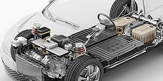
The shift in production to electric vehicles, expansion of services promoted by commercialized 5G, and recovery of capital investment in data centers are all signs of ever-increasing growth in the semiconductor market.
As this market is expected to show constant growth over time, Mitutoyo, as a solution provider and metrology expert, is ready to provide measurement solutions for various electronic manufacturing processes.
Need more information?
Please get in touch
Contact us to find out more about Mitutoyo's Quality assurance in the Electronics Industry
Common Parts Passing Through Quality Assurance in the Electronics Industry
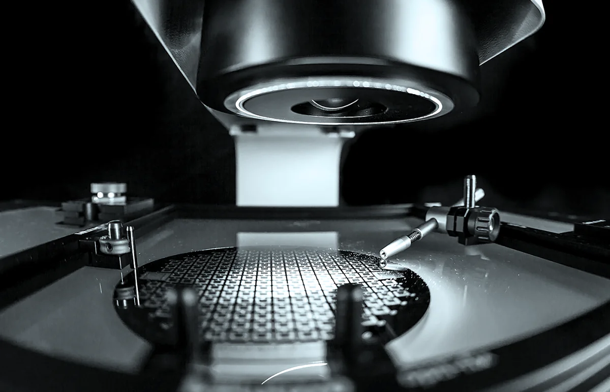
Semiconductors / Wafers
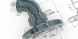
Semiconductors are an essential component of modern electronics, used in many devices you see on a daily basis. The manufacturing of semiconductors involves a complex process of layering materials on a wafer of silicon, followed by precision cutting and shaping to create individual chips.
One of the most critical steps in semiconductor production is the cutting of said wafers, as it determines the size and shape of each chip. Various techniques are used for wafer cutting, including mechanical sawing, laser cutting, and plasma cutting. This is a process that must be highly precise and accurate to ensure that each chip is identical and functional.
Quality Control Techniques


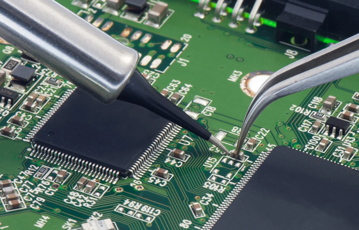
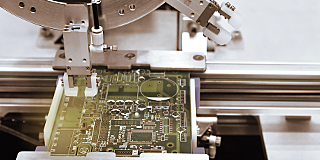
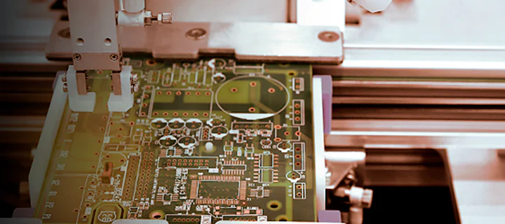
PCB / Soldering Pins / Wire Bonding
Printed Circuit Boards (PCBs) are a necessary component in electronic devices, providing a platform for connecting various components.
Soldered onto the PCBs to ensure stable electrical connections, pins are the channel through which communication can take place. Soldering pins requires careful attention to temperature, solder composition, and other factors to ensure this strong and reliable connection.
Wire bonding is another well-known process in the electronics industry, used to connect semiconductor devices between each other and to the leads of an integrated circuit. The quality of these connections is of the utmost importance if they are expected to perform as intended.
Quality Control Techniques


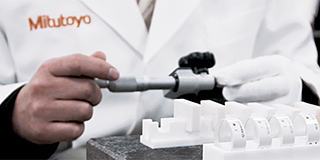
Cables / Connectors
Cables come in various types, including coaxial, twisted pair, and optical fiber, and are used to transmit data and power between devices. And connectors are used to join these cables together or connect them to devices directly. They come in many forms with the most common being USB, HDMI, and RJ45. As there are set specifications and standards for cables and connectors to ensure they operate accordingly, quality control is of the highest importance.
Quality Control Techniques


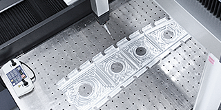
TOP SELLING PRODUCTS FOR ELECTRONICS
Our advanced CMM systems, laser-optical scanning technology and software analysis techniques are ideal for the 3D measurement necessary for complex electronics applications.